US 11,967,364 B2
Variable width memory module supporting enhanced error detection and correction
Frederick A. Ware, Los Altos Hills, CA (US); John Eric Linstadt, Palo Alto, CA (US); and Kenneth L. Wright, Sunnyvale, CA (US)
Assigned to Rambus Inc., San Jose, CA (US)
Filed by Rambus Inc., San Jose, CA (US)
Filed on May 30, 2023, as Appl. No. 18/203,511.
Application 18/203,511 is a continuation of application No. 17/501,311, filed on Oct. 14, 2021, granted, now 11,705,187.
Application 17/501,311 is a continuation of application No. 17/101,574, filed on Nov. 23, 2020, granted, now 11,164,622, issued on Nov. 2, 2021.
Application 17/101,574 is a continuation of application No. 16/856,596, filed on Apr. 23, 2020, granted, now 10,878,888, issued on Dec. 29, 2020.
Application 16/856,596 is a continuation of application No. 16/440,015, filed on Jun. 13, 2019, granted, now 10,650,881, issued on May 12, 2020.
Application 16/440,015 is a continuation of application No. 16/011,539, filed on Jun. 18, 2018, granted, now 10,339,999, issued on Jul. 2, 2019.
Application 16/011,539 is a continuation of application No. 15/610,001, filed on May 31, 2017, granted, now 10,014,047, issued on Jul. 3, 2018.
Application 15/610,001 is a continuation of application No. 15/262,741, filed on Sep. 12, 2016, granted, now 9,697,884, issued on Jul. 4, 2017.
Claims priority of provisional application 62/239,158, filed on Oct. 8, 2015.
Prior Publication US 2023/0377632 A1, Nov. 23, 2023
Int. Cl. G11C 7/10 (2006.01); G06F 11/10 (2006.01); G11C 7/02 (2006.01); G11C 11/4093 (2006.01); G11C 11/4096 (2006.01); G11C 29/52 (2006.01); G11C 29/04 (2006.01)
CPC G11C 11/4093 (2013.01) [G06F 11/1048 (2013.01); G11C 7/02 (2013.01); G11C 11/4096 (2013.01); G11C 29/52 (2013.01); G11C 2029/0411 (2013.01)] 20 Claims
OG exemplary drawing
 
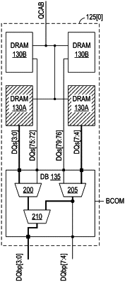
1. A data-buffer component comprising:
a primary data port to couple to a memory-controller component;
first and second secondary data ports to couple to respective first and second memory components; and
data-buffer component supporting a first access mode and a second access mode, wherein:
in the first access mode, the data-buffer component communicates, to the primary data port, first data bursts from the first secondary data port separate from second data bursts from the second secondary data port; and
in the second access mode, the data-buffer component simultaneously receives ones of the first data bursts from the first secondary data port and ones of the second data bursts from the second secondary data port and communicates, to the primary data port, the ones of the first data bursts from the first secondary data port interleaved with the ones of the second data bursts from the second secondary data port.