| CPC G11C 11/4093 (2013.01) [G09G 3/2096 (2013.01); G09G 3/3208 (2013.01); G11C 11/4076 (2013.01); G11C 11/419 (2013.01); G09G 2330/021 (2013.01); G09G 2330/04 (2013.01)] | 16 Claims |
|
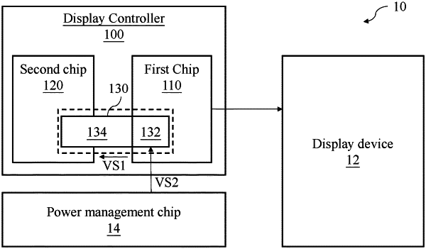
1. A display controller comprising:
a first chip, configured to control a display device;
a second chip, externally coupled to the first chip, and configured to be a random access memory; and
a protection circuit, comprising a first portion and a second portion, and the second portion comprising a first circuit, a second circuit, and a third circuit;
wherein the first chip is further configured to provide a first supply power to the second chip according to a second supply power received externally and to access the second chip during the controlling of the display device;
wherein the protection circuit is configured to reduce an effect of a sur e of the second supply power on the first supply power, the first portion is configured to be an electrostatic discharge (ESD) circuit and formed in the first chip, and the second portion is configured to be a low pass filter and coupled to the first chip and the second chip; and
wherein the first chip at least comprises a first pad, a second pad, and a third pad, the second chip at least comprises a fourth pad and a fifth pad, the first pad is arranged to receive the second supply power, the fourth pad is arranged to receive the first supply power, the first portion is coupled between the first pad and the second pad, the first circuit is coupled between the first pad and the third pad, the second circuit is coupled between the third pad and the fourth pad, and the third circuit is coupled between the fourth pad and the fifth pad.
|