| CPC G09G 3/3233 (2013.01) [G09G 3/3266 (2013.01); G09G 3/3291 (2013.01); G09G 2300/0852 (2013.01); G09G 2310/061 (2013.01); G09G 2320/0233 (2013.01)] | 13 Claims |
|
1. A pixel driving circuit for driving a light-emitting element to emit light, comprising: a drive transistor, a light emission control transistor, a first capacitor, a second capacitor, a reset circuit, a data write circuit, and a threshold compensation circuit; wherein
a gate of the drive transistor, a first terminal of the first capacitor, a second terminal of the second capacitor, and the threshold compensation circuit are electrically connected to a first node; a first terminal of the second capacitor is configured to receive a fixed voltage signal; a first electrode of the light emission control transistor, a second electrode of the drive transistor, and the threshold compensation circuit are electrically connected to a second node; a second electrode of the light emission control transistor, the reset circuit, and an anode of the light-emitting element are electrically connected to a third node;
wherein the reset circuit comprises a reset transistor, and the threshold compensation circuit comprises a threshold compensation transistor, and the data write circuit comprises a data write transistor;
a first electrode of the reset transistor is configured for receiving a reset signal, a second electrode of the reset transistor is electrically connected to the third node, and a gate of the reset transistor is configured for receiving a second scan signal and is configured to be turned on or off under control of the second scan signal; and
a gate of the threshold compensation transistor is configured for receiving a first scan signal, a first electrode of the threshold compensation transistor is electrically connected to the first node, and a second electrode of the threshold compensation transistor is electrically connected to the second node and is configured to be turned on or off under control of the first scan signal;
a gate of the data write transistor is configured for receiving a third scan signal and configured to be turned on or off under control of the third scan signal, a first electrode of the data write transistor is electrically connected to a second terminal of the first capacitor through a fourth node, and a second electrode of the data write transistor is configured for receiving a data signal;
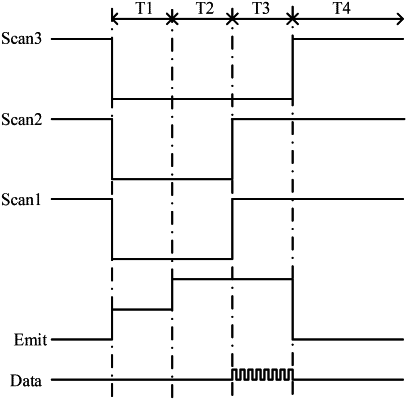
at an initial stage, the reset circuit is configured to provide the reset signal to the third node to reset the anode of the light-emitting element; the light emission control transistor is configured to be in a first on state under control of a first light emission enable level to transmit the reset signal to the second node to reset the second electrode of the drive transistor; when the first scan signal is applied to the threshold compensation transistor, the threshold compensation transistor is configured to transmit the reset signal to the first node to reset the first capacitor, the second capacitor, and the gate of the drive transistor; and the data write transistor is configured to transmit a non-enable level of the data signal to the second terminal of the first capacitor;
at a threshold compensation stage, the threshold compensation transistor is configured to provide a threshold voltage of the drive transistor to the first node for compensation such that a potential of the first node is equal to VN1; and the data write transistor is configured to continue writing the non-enable level of the data signal to the second terminal of the first capacitor, and the reset transistor is further configured to continuously provide the reset signal to the third node;
at a data write stage, the data write transistor is configured to write an enable level of the data signal to the second terminal of the first capacitor such that the potential of the first node changes from VN1 to VN1′, wherein VN1′=VN1−(Vdata−Vofs)×(c1/(c1+c2)), Vdata denotes the enable level of the data signal, Vofs denotes the non-enable level of the data signal, c1 denotes a capacitance value of the first capacitor, and c2 denotes a capacitance value of the second capacitor; and
at a light emission stage, the light emission control transistor is configured to be in a second on state under control of a second light emission enable level such that a drive current generated by the drive transistor according to the potential VN1′ of the first node is transmitted to the light-emitting element to drive the light-emitting element to emit light;
wherein a smaller current flows through the light emission control transistor in the first on state than the light emission control transistor in the second on state,
wherein the pixel driving circuit further comprises: a signal conversion circuit electrically connected to a gate of the light emission control transistor; wherein the signal conversion circuit is configured to provide:
at the initial stage, the first light emission enable level to the gate of the light emission control transistor to control the light emission control transistor to be in the first on state,
at the threshold compensation stage and the data write stage, a light emission non-enable level to the gate of the light emission control transistor to control the light emission control transistor to be in an off state, and
at the light emission stage, the second light emission enable level to the gate of the light emission control transistor to control the light emission control transistor to be in the second on state.
|