| CPC G09G 3/32 (2013.01) [G09G 3/2007 (2013.01); G09G 2320/02 (2013.01); G09G 2330/028 (2013.01)] | 9 Claims |
|
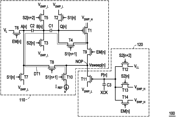
1. A sweep voltage generator, comprising:
an output node, used to provide a sweep signal;
a current generating circuit, coupled to the output node, comprising a detection path for detecting an output load variation on the output node, and adjusting the sweep signal provided by the output node based on the output load variation; and
a voltage regulating circuit, coupled to the output node for regulating a voltage the output node,
wherein a current flowing through the output node is set based on the output load variation, and
wherein the current generating circuit comprises:
a first transistor, having a first terminal receiving a swing high voltage, a control terminal, and a second terminal;
a second transistor, having a first terminal receiving a swing low voltage, a control terminal receiving a first control signal, and a second terminal coupled to the control terminal of the first transistor;
a third transistor, having a first terminal, a control terminal receiving a second control signal, and a second terminal receiving the swing low voltage;
a first capacitor, coupled between the second terminal of the second transistor and the first terminal of the third transistor;
a fourth transistor, having a first terminal coupled to the second terminal of the first transistor, a control terminal receiving a third control signal, and a second terminal coupled to the control terminal of the first transistor;
a fifth transistor, having a first terminal receiving the swing low voltage, a control terminal receiving a fourth control signal, and a second terminal;
a sixth transistor, having a first terminal, a control terminal receiving a light emission control signal, and a second terminal receiving a low voltage;
a second capacitor, coupled between the first terminal of the third transistor and the first terminal of the sixth transistor;
a seventh transistor, having a first terminal coupled to the first terminal of the sixth transistor, a control terminal receiving the first control signal, and a second terminal receiving the swing low voltage;
an eighth transistor, having a first terminal coupled to the output node, a control terminal receiving the third control signal, and a second terminal coupled to the first terminal of the sixth transistor;
a ninth transistor, having a first terminal coupled to the second terminal of the first transistor, a control terminal receiving the light emission control signal, and a second terminal coupled to the output node;
a tenth transistor, having a first terminal coupled to the output node, a control terminal receiving the third control signal, and a second terminal; and
a current source, coupled to the second terminal of the tenth transistor.
|