| CPC G09G 3/2074 (2013.01) [G09G 2300/0443 (2013.01); G09G 2300/0452 (2013.01); G09G 2320/0233 (2013.01); G09G 2320/0242 (2013.01); G09G 2320/028 (2013.01); G09G 2360/16 (2013.01)] | 21 Claims |
|
1. A display device comprising:
a communication interface comprising a circuit;
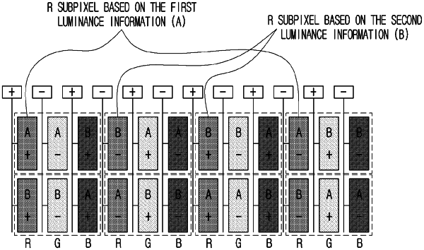
a display panel comprising a plurality of pixels, the plurality of pixels comprising red (R), green (G), and blue (B) subpixels;
a memory configured to store first luminance information and second luminance information; and
a processor configured to:
acquire, based on the first luminance information, a luminance value corresponding to at least one of a plurality of subpixel values included in an input frame received via the communication interface,
acquire, based on the second luminance information, a luminance value corresponding to the remaining of the plurality of subpixel values,
based on the acquired luminance values, acquire an output frame, and
control the display panel to output the output frame,
wherein the processor is further configured to:
group the plurality of pixels into a plurality of groups each including a number of pixels such that each group of the plurality of groups comprises R subpixels, G subpixels, and B subpixels, and
at least one of:
apply a voltage of a first polarity to at least one R subpixel of the R subpixels and apply a voltage of a second polarity to the remaining R subpixels of the R subpixels,
apply a voltage of the first polarity to at least one G subpixel of the G subpixels and apply a voltage of the second polarity to the remaining G subpixels of the G subpixels, and
apply a voltage of the first polarity to at least one B subpixel of the B subpixels and apply a voltage of the second polarity to the remaining B subpixels of the B subpixels.
|