| CPC G06F 3/0655 (2013.01) [G06F 3/0604 (2013.01); G06F 3/0673 (2013.01)] | 16 Claims |
|
1. A memory device, comprising:
a memory array, for storing a plurality of vector data, the vector data at least include an input feature vector and an output feature vector, each vector data has an MSB vector and a LSB vector, comprising:
a plurality of memory units, each memory unit has a first bit and a second bit, the first bit is used to store the MSB vector of each vector data, and the second bit is used to store the LSB vector of each vector data,
and
a plurality of data latches, comprising:
a first data latch;
a second data latch; and
a common data latch,
wherein a bit line corresponding to each vector data executes one time of bit-line-setup, and reads the MSB vector and the LSB vector of each vector data according to the bit line, the threshold voltage distribution of each memory unit is divided into N states, N is a positive integer and N is less than 2 to the power of 2, and the effective bit number stored by each memory unit is less than 2; and
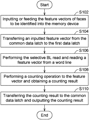
wherein the common data latch receives the input feature vector from the memory device externally, then the input feature vector is transferred from the common data latch and then temporarily stored to the first data latch, the memory device executes a selective bit line read operation based on the input feature vector in the first data latch to read the MSB vector and the LSB vector of the input feature vector according to the corresponding bit line which have been performed with the bit-line-setup, so as to obtain the output feature vector, then the output feature vector is temporarily stored in the second data latch.
|