| CPC G06F 3/0655 (2013.01) [G06F 3/0604 (2013.01); G06F 3/0679 (2013.01)] | 12 Claims |
|
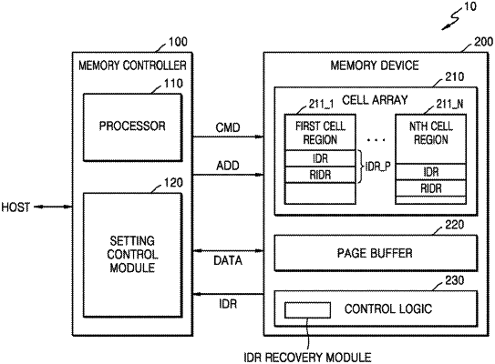
1. A memory device comprising:
a cell array including a plurality of cell blocks, each cell block including a plurality of pages; and
a control logic configured to control a program and read operation on the cell array, wherein:
at least one page of the cell array stores information data read (IDR) data that includes information related to a setting operation of the memory device, and at least one other page of the cell array stores replica IDR data including inverted bit values of the IDR data;
the IDR data and the replica IDR data constitute one IDR data pair;
a plurality of IDR data pairs is stored in the cell array;
the control logic is configured to, when a read fail of the IDR data occurs:
control a recovery operation for repairing errors in the IDR data by reading the replica IDR data,
control the read operation so that the plurality of IDR data pairs is read, and
based on the plurality of read IDR data pairs, perform the recovery operation for repairing the errors that have occurred in the IDR data; and
wherein the control logic is further configured to determine a bit value of each bit of the IDR data based on a majority rule with respect to bit values determined from each of the plurality of read IDR data pairs.
|