US 11,966,616 B2
Voltage bin calibration based on a voltage distribution reference voltage
Kishore Kumar Muchherla, San Jose, CA (US); Devin M. Batutis, San Jose, CA (US); Xiangang Luo, Fremont, CA (US); Mustafa N. Kaynak, San Diego, CA (US); Peter Feeley, Boise, ID (US); Sivagnanam Parthasarathy, Carlsbad, CA (US); Sampath Ratnam, Boise, ID (US); and Shane Nowell, Boise, ID (US)
Assigned to Micron Technology, Inc., Boise, ID (US)
Filed by MICRON TECHNOLOGY, INC., Boise, ID (US)
Filed on Feb. 27, 2023, as Appl. No. 18/175,439.
Application 18/175,439 is a continuation of application No. 17/203,474, filed on Mar. 16, 2021, granted, now 11,620,074.
Prior Publication US 2023/0205447 A1, Jun. 29, 2023
This patent is subject to a terminal disclaimer.
Int. Cl. G06F 3/00 (2006.01); G06F 3/06 (2006.01)
CPC G06F 3/0653 (2013.01) [G06F 3/0604 (2013.01); G06F 3/0655 (2013.01); G06F 3/0679 (2013.01)] 20 Claims
OG exemplary drawing
 
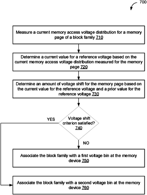
1. A method comprising:
determining a current value for a reference voltage for a block family of a memory device;
determining an amount of voltage shift for a memory page of the block family based on the current value for the reference voltage and a prior value for the reference voltage; and
associating the block family with a first voltage bin of a plurality of voltage bins or a second voltage bin of the plurality of voltage bins based on the determined amount of voltage shift, wherein the first voltage bin is associated with a first voltage offset and the second voltage bin is associated with a second voltage offset.