| CPC G06F 3/044 (2013.01) [G02F 1/1677 (2019.01)] | 16 Claims |
|
1. A display device, comprising:
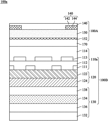
a base layer comprising a colorless polyimide (CPI) layer and a water vapor barrier layer;
a touch sensing layer disposed on the base layer and comprising a second insulating layer;
a light guide module disposed on the touch sensing layer, wherein the light guide module comprises a light guide plate and a cover structure, the light guide plate comprises a dot structure, and the light guide plate and the cover structure have no adhesive material therebetween, and a material of the light guide plate comprises thermoplastic polyurethanes (TPU);
a display panel, wherein the touch sensing layer is located between the light guide module and the display panel, and the touch sensing layer and the display panel have no adhesive material therebetween, the display panel comprises a substrate, an electronic ink layer, a lower electrode, and an upper electrode, the upper electrode contacts a surface of the water vapor barrier layer facing away from the colorless polyimide layer, and the upper electrode is located between the electronic ink layer and the water vapor barrier layer; and
an adhesive layer disposed between the light guide module and the touch sensing layer, wherein the adhesive layer contacts and adheres the dot structure of the light guide plate and the second insulating layer of the touch sensing layer.
|