| CPC G06F 3/04184 (2019.05) [G06F 3/0412 (2013.01); G06F 3/0444 (2019.05); G06F 3/0446 (2019.05); G09G 3/3208 (2013.01); G06F 2203/04107 (2013.01); G06F 2203/04112 (2013.01)] | 20 Claims |
|
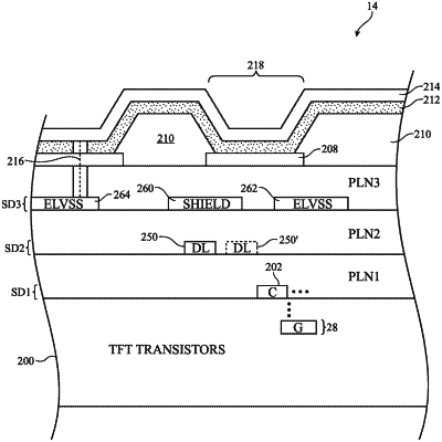
1. Display circuitry comprising:
a transistor having a gate conductor;
a first planarization layer formed over the gate conductor;
one or more contacts formed in a first source-drain routing layer within the first planarization layer;
a second planarization layer formed on the first planarization layer;
one or more data lines formed in a second source-drain routing layer within the second planarization layer;
a third planarization layer formed on the second planarization layer; and
a data line shielding conductor formed in a third source-drain routing layer within the third planarization layer, the data line shielding conductor disposed directly over the one or more data lines.
|