| CPC G06F 3/0418 (2013.01) [G02F 1/13338 (2013.01); G06F 3/044 (2013.01); G02F 1/133308 (2013.01)] | 14 Claims |
|
1. A compensation circuit applicable to a touch screen and comprising a logic circuit, a selection circuit, and a switch circuit, wherein
the logic circuit is configured to obtain a first selection signal, a second selection signal, and a third selection signal according to an enable signal and a timing signal;
the selection circuit is configured to obtain a first control signal, a second control signal, and a third control signal according to the first selection signal, the second selection signal, and the third selection signal;
the switch circuit is configured to be switched on in response to the first control signal to transmit a common voltage signal to a common electrode of the touch screen, be switched on in response to the second control signal to transmit a first compensation voltage signal to the common electrode, and be switched on in response to the third control signal to transmit a second compensation voltage signal to the common electrode;
the switch circuit comprises a first switch unit, a second switch unit, and a third switch unit, wherein the first switch unit is configured to be switched on under control of the first control signal to transmit the common voltage signal to the common electrode, the second switch unit is configured to be switched on under control of the second control signal to transmit the first compensation voltage signal to the common electrode, and the third switch unit is configured to be switched on under control of the third control signal to transmit the second compensation voltage signal to the common electrode;
when any one of the first switch unit corresponding to the first control signal, the second switch unit corresponding to the second control signal, and the third switch unit corresponding to the third control signal is switched on, the other two are switched off; and
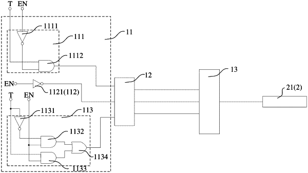
the logic circuit comprises a first processing module, wherein the first processing module comprises a first inverter circuit and a first AND gate circuit, and wherein the first inverter circuit has an input terminal configured to receive the enable signal and an output terminal electrically coupled with a first terminal of the first AND gate circuit, and the first AND gate circuit has a second terminal configured to receive the timing signal and an output terminal configured to output the first selection signal to the selection circuit.
|