| CPC G06F 21/755 (2017.08) [G06F 21/51 (2013.01); G06F 21/554 (2013.01); G06F 21/81 (2013.01); H04L 12/40013 (2013.01); H04L 2012/40215 (2013.01); H04L 2012/40267 (2013.01); H04L 2012/40273 (2013.01); H04L 63/1416 (2013.01)] | 22 Claims |
|
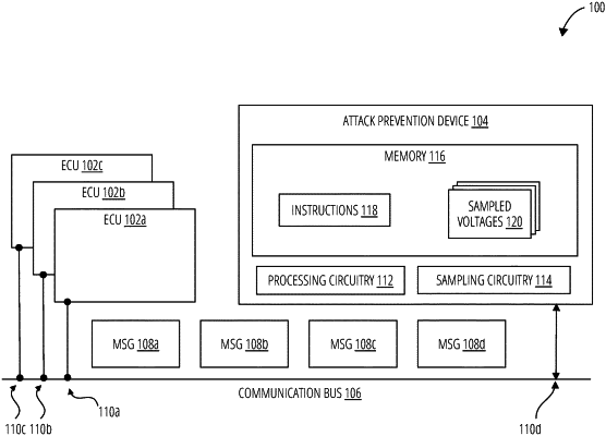
8. A system, comprising:
a communication bus;
circuitry; and
memory storing instructions that, when executed by the circuitry, cause the circuitry to:
sample a voltage waveform on the communication bus;
identify a glitch in the voltage waveform; and
modify the voltage level on the communication bus based on the glitch to force bit levels to remain constant through an entire bit width of the glitch.
|