| CPC G06F 13/1668 (2013.01) [G06F 15/8038 (2013.01)] | 20 Claims |
|
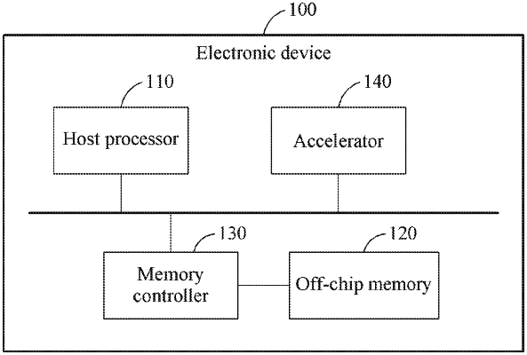
1. An accelerator comprising:
a memory configured to store input data;
a plurality of shift buffers each configured to
shift input data received sequentially from the memory in each cycle, and
in response to input data being stored in each of internal elements of the shift buffer, output the stored input data to a processing element (PE) array;
a plurality of backup buffers each configured to store input data received sequentially from the memory, and transfer the stored input data to one of the shift buffers in response to all data included in a row of the input data being output to the PE array through the one of the shift buffers; and
the PE array configured to perform an operation on input data received from one or more of the shift buffers and on a corresponding kernel.
|