| CPC G06F 11/1044 (2013.01) [G06F 11/1072 (2013.01); G11C 11/4096 (2013.01)] | 20 Claims |
|
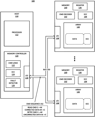
1. A memory device comprising:
a hardware interface to receive a first read command for an address from a host; and
on-die error checking and correction (ECC) circuitry to receive read data, process the read data internally to the memory device with the on-die ECC circuitry to generate ECC processed read data, and return the ECC processed read data from the address to the host in response to the first read command, wherein in response to detection of a detected, uncorrectable error (DUE) by the on-die ECC circuitry, the on-die ECC circuitry is also to return a DUE indication to the host in response to the first read command;
wherein the hardware interface is to receive a second read command from the host to the address subsequent to the first read command, in response to the DUE indication; and
wherein the second read command is to disable application of the on-die ECC circuitry, to trigger the memory device to return the read data from the address not processed by the on-die ECC circuitry in response to the second read command.
|