| CPC G03F 7/70633 (2013.01) [G03F 7/70775 (2013.01); G03F 7/70783 (2013.01); G03F 9/7003 (2013.01); G03F 9/7046 (2013.01); G03F 9/7073 (2013.01); G03F 9/7088 (2013.01); H01L 21/682 (2013.01)] | 20 Claims |
|
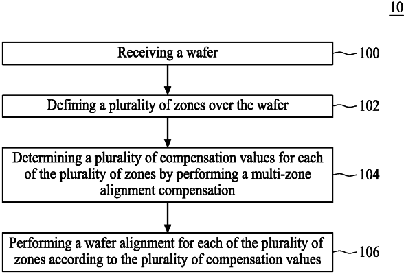
1. A method comprising:
receiving a wafer;
measuring a surface topography of the wafer;
calculating a topographical variation based on the surface topography measurement;
performing a single-zone alignment compensation when the topographical variation is less than a predetermined value, or performing a multi-zone alignment compensation when the topographical variation is greater than the predetermined value; and
performing a wafer alignment according to the single-zone alignment compensation or the multi-zone alignment compensation,
wherein the multi-zone alignment compensation further comprises:
defining a plurality of zones over the wafer, wherein each zone includes a plurality of fields; and
performing the multi-zone alignment compensation for each of the plurality of zones by a controller according to an equation (1),
wherein the equation (1) is:
dXm=αm*Z1+βm*Z2+γm*Z3+ . . . ωm*Zn (1)
wherein n is a positive integer greater than 1, m indicates that the zone undergoes the multi-zone alignment compensation and m is a positive integer less than or equal to n, dXm indicates the compensation value to be adjusted during the wafer alignment, Z1 to Zn indicate a first zone to an Nth zone of the plurality of zones, αm indicates a weighting for the fields in the first zone during performing of the multi-zone alignment compensation for an mth zone, βm indicates a weighting for the fields in the second zone during performing of the multi-zone alignment compensation for the mth zone, γm indicates a weighting for the fields in the third zone during performing of the multi-zone alignment compensation for the mth zone, and ωm indicates a weighting for the fields in the Nth zone during performing of the multi-zone alignment compensation for the mth zone.
|