| CPC G02F 1/136286 (2013.01) [G02F 1/136222 (2021.01); G02F 1/136213 (2013.01)] | 20 Claims |
|
1. An array substrate, comprising:
a base substrate; and
a plurality of pixel electrodes, a plurality of first common electrodes, a first-common-signal line and a connection line, disposed on the base substrate;
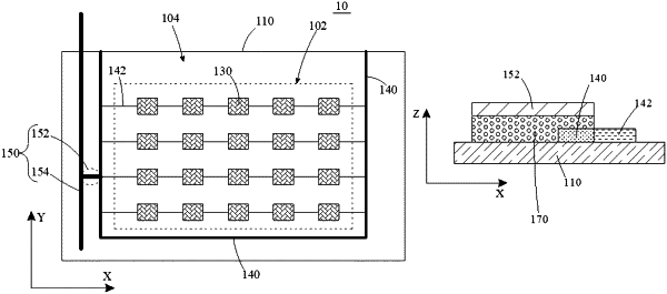
wherein the array substrate comprises a first region and a second region surrounding the first region along an extending direction of the base substrate, the plurality of pixel electrodes and the plurality of first common electrodes are located in the first region, and one of the plurality of first common electrodes is configured to be coupled with one of the plurality of pixel electrodes to form a capacitor, the first-common-signal line is located in the second region, a first end of the connection line is connected with the first-common-signal line, and a second end of the connection line is connected with the plurality of first common electrodes; and
wherein the array substrate further comprises a detection line, a portion of the detection line is located in the second region, and the other portion of the detection line is extended outside the base substrate, the detection line and the first-common-signal line are insulated from each other, and an orthographic projection of the detection line on the base substrate and an orthographic projection of the first-common-signal line on the base substrate have at least one intersection point.
|