| CPC G02B 13/0015 (2013.01) [G02B 1/041 (2013.01); G02B 1/11 (2013.01); G02B 5/003 (2013.01); H04N 23/51 (2023.01); H04N 23/57 (2023.01)] | 20 Claims |

|
1. An electronic device comprising:
a housing; and
a camera disposed in an inner space of the housing,
wherein the camera comprises:
an image sensor, and
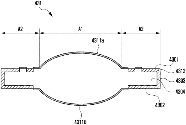
a plurality of lenses aligned with the image sensor, wherein each of the plurality of lenses comprising a first surface, a second surface directed in an opposite direction to the first surface and a lens side surface surrounding a space between the first surface and the second surface, and
wherein the each of the plurality of lenses comprises:
a first area formed to transfer at least a part of an external light to the image sensor, and
a second area including a light absorbing layer formed to absorb the at least a part of the external light and to penetrate from an outer surface of the each of the plurality of lenses into the space, and
wherein the light absorbing layer is formed via a coloring liquid penetrating from the outer surface of the each of the plurality of lenses into the space, and
wherein the light absorbing layer is formed from the first surface, the second surface and the lens side surface into at least a part of the space in the second area.
|