| CPC G01S 7/4863 (2013.01) [G01S 17/89 (2013.01); H01L 25/042 (2013.01); H01L 25/043 (2013.01); H01L 31/107 (2013.01)] | 14 Claims |
|
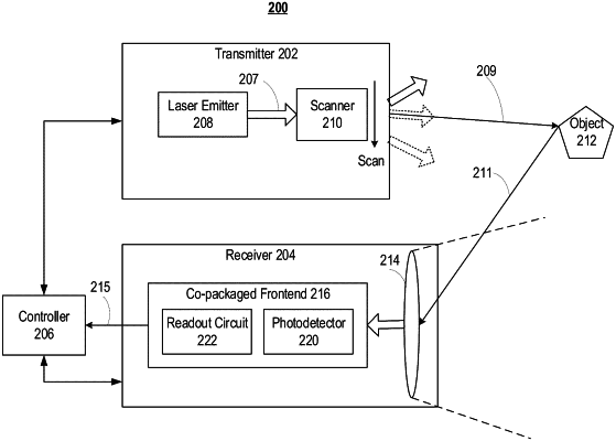
1. An optical sensing system, comprising:
a light source configured to emit an optical signal into an environment surrounding the optical sensing system;
a photodetector configured to receive the optical signal reflected from the environment of the optical sensing system, and convert the optical signal to an electrical signal, the photodetector being disposed in a substrate;
a readout circuit configured to generate a readout signal based on the electrical signal received from the photodetector, the readout circuit being disposed in the same substrate as the photodetector and connected to the substrate through one or more bonding,
wherein the photodetector and the readout circuit are stacked over one another, and are connected through one or more through silicon vias (TSVs) in a three-dimensional (3D) structure.
|