| CPC G01N 21/9501 (2013.01) [G01N 21/8806 (2013.01); G06T 7/0004 (2013.01); G06T 2207/30148 (2013.01)] | 17 Claims |
|
1. A system comprising:
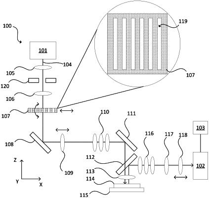
a light source that generates a beam of light;
an objective;
a chuck configured to hold a wafer in a path of the beam of light that passes through the objective;
a tunable illumination aperture disposed in the path of the beam of light between the light source and the objective;
a first movable focus lens disposed in the path of the beam of light between the light source and the objective;
a 2D imaging camera configured to capture a wafer image in an illuminated area through the objective;
a second movable focus lens disposed in the path of the beam of light between the objective and the 2D imaging camera; and
wherein the first movable focus lens and the second movable focus lens are configured to adjust an illumination conjugate between the light source and the wafer and a collection conjugate between the wafer and the 2D imaging camera, and wherein the first movable focus lens and the second movable focus lens are configured to position an illumination focus at, above, or below a surface of the wafer; and
wherein the 2D imaging camera is configured to generate a gray field image of the wafer.
|