| CPC G01L 9/065 (2013.01) [B81C 1/00539 (2013.01); B81C 2201/0133 (2013.01); B81C 2201/016 (2013.01); B81C 2201/0171 (2013.01)] | 7 Claims |
|
1. A bipolar transistor type MEMS pressure sensor, including:
a thin film, suspended on a substrate through a supporting structure, and configured to deform in different degrees according to pressure suffered;
a cantilever beam, disposed on the side face of the thin film and suspended on the supporting structure through the thin film;
a bipolar transistor, including a base region, a collector region and an emitter region, the collector region and the emitter region are disposed on the cantilever beam, the base region is disposed at a position, close to the supporting structure, of the thin film, the base region includes a sensing area and a connecting area, the sensing area is disposed on the thin film and is respectively connected to the collector region and the emitter region through the connecting area, and the base region is configured to sense the deformation of the thin film through a change in resistance value;
a preparation method of the bipolar transistor type MEMS pressure sensor includes:
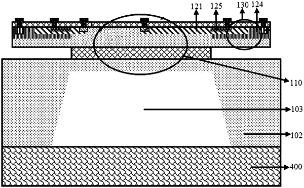
providing a substrate, the substrate includes a first structural layer, a second structural layer disposed on the first structural layer, and a third structural layer disposed on the second structural layer along a thickness direction, and the substrate is provided with a first surface and a second surface, the first surface is provided with a compression area;
doping on the first surface to form a bipolar transistor, the bipolar transistor includes a base region, a collector region, and an emitter region, the base region is located within the pressure region and is respectively connected to the collector region and the emitter region; etching and forming a concave cavity at a corresponding position of the pressure area on the second surface to form a thin film on the substrate corresponding to the concave cavity; the cavity is formed in the first structural layer, and defines the first structural layer as a first thin film layer and a supporting structure supporting the first thin film layer;
etching the second structural layer to form a supporting layer, the supporting layer is overlapped with the first thin film layer, and defines the third structural layer as a second thin film layer overlapped with the supporting layer and a cantilever beam connected to the second thin film layer, and the collector region and the emitter region are located on the cantilever beam;
bonding the second surface with the substrate to form the bipolar transistor type MEMS pressure sensor.
|