| CPC F21K 9/90 (2013.01) [F21Y 2103/10 (2016.08); F21Y 2115/10 (2016.08)] | 14 Claims |
|
1. A method for manufacturing a light-emitting diode (LED) strip, comprising:
arranging at least two conductive lines to extend along a first linear trace, spacing being present between two adjacent ones of the conductive lines; and
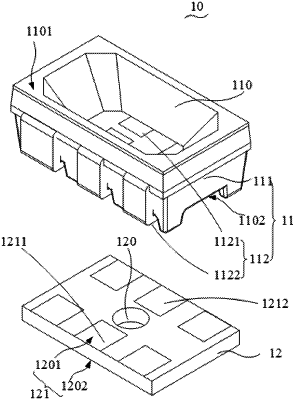
arranging at least two supporting bases at intervals along the first linear trace on the at least two conductive lines; wherein each of the supporting bases comprises multiple conductive portions and at least one avoidance through-hole; each two of the multiple conductive portions being arranged at intervals along the first linear trace, the at least one avoidance through-hole being disposed between two of the multiple conductive portions arranged along the first linear trace;
subjecting the supporting bases and the conductive lines to processing of soldering, so as to have each of the conductive lines soldered to two of the conductive portions that are arranged along the first linear trace, and a portion of at least one of the conductive lines spanning over one of the at least one avoidance through-hole located between two of the conductive portions that are arranged along the first linear trace to form a spanning portion;
subjecting the spanning portion to processing of stamp-cutting so as to cut off the conductive line through stamping;
disposing at least one LED bead on a surface of each of the supporting bases that faces away from the conductive lines, wherein each of the LED beads comprises a plurality of pin portions each corresponding to one of the conductive portions; and
subjecting the pin portions and the conductive portions to processing of soldering,
wherein the method further comprises processing the at least two conductive lines to strip off insulation layers thereof so that each of the conductive lines is formed with a line core exposed portion corresponding to one of the supporting bases, and each of the line core exposed portions is connected to two of the conductive portions, that are arranged along the first linear trace, of a corresponding one of the supporting bases; when the supporting bases are soldered to the at least two conductive lines, each of the line core exposed portions is soldered to the two conductive portions arranged along the first linear trace, and at least one of the line core exposed portions spans over the avoidance through-hole which is located between the two conductive portions arranged along the first linear trace, to form the spanning portion.
|