US 11,965,268 B2
Group 13 element nitride wafer with reduced variation in off-cut angle
Vianney Leroux, Antibes (FR); Vincent Gelly, Valbonne (FR); Nabil Nahas, Mougins (FR); and Kevin Provost, Le Luc en Provence (FR)
Assigned to IV WORKS CO., LTD., (KR)
Appl. No. 17/774,690
Filed by IV WORKS CO., LTD, Daejeon (KR)
PCT Filed Nov. 5, 2020, PCT No. PCT/FR2020/052004
§ 371(c)(1), (2) Date May 5, 2022,
PCT Pub. No. WO2021/089947, PCT Pub. Date May 14, 2021.
Claims priority of application No. 1912414 (FR), filed on Nov. 5, 2019.
Prior Publication US 2022/0282397 A1, Sep. 8, 2022
Int. Cl. C30B 25/02 (2006.01); C30B 29/40 (2006.01); C30B 33/08 (2006.01)
CPC C30B 29/406 (2013.01) [C30B 25/02 (2013.01); C30B 33/08 (2013.01)] 18 Claims
OG exemplary drawing
 
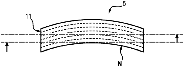
1. Two-dimensional crystal wafer of group 13 or III element nitride, delimited by a face of orientation N, an opposite face of orientation E according to the group 13 or III element, E being chosen preferably from Ga, In, Al or a combination of these elements:
wherein:
the variation of the crystalline off-cut angle along the largest dimension of said wafer is less than 5×10⁻³°/mm, and
its geometric curvature or deformation of its faces has a deflection less in absolute value than 10−3 mm/mm of the largest dimension of said wafer.