US 11,964,472 B2
Applying marks to a surface of a medium
Li Qian, Sant Cugat del Valles (ES); Diego Lopez Ubieto, Sant Cugat del Valles (ES); and Francisco Guerrero Carvajal, Sant Cugat del Valles (ES)
Assigned to Hewlett-Packard Development Company, L.P., Spring, TX (US)
Appl. No. 17/261,048
Filed by Hewlett-Packard Development Company, L.P., Spring, TX (US)
PCT Filed Nov. 28, 2018, PCT No. PCT/US2018/062720
§ 371(c)(1), (2) Date Jan. 18, 2021,
PCT Pub. No. WO2020/112097, PCT Pub. Date Jun. 4, 2020.
Prior Publication US 2021/0323324 A1, Oct. 21, 2021
Int. Cl. B41J 11/46 (2006.01); B41J 11/42 (2006.01); B41J 11/44 (2006.01); G01P 3/38 (2006.01); G06V 10/22 (2022.01)
CPC B41J 11/46 (2013.01) [B41J 11/42 (2013.01); B41J 11/44 (2013.01); G01P 3/38 (2013.01); G06V 10/225 (2022.01)] 8 Claims
OG exemplary drawing
 
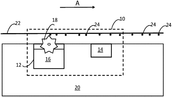
1. An optical sensor device, comprising:
an application module for applying an irregular pattern of marks to a surface of a medium; and
an optical detector module for acquiring images of the applied marks and for determining an advancement speed of the medium based on the acquired images,
wherein the application module comprises a reservoir and an application device that is in contact with marking fluid provided in the reservoir and with the medium.