| CPC B32B 7/14 (2013.01) [B32B 37/12 (2013.01); B60K 35/00 (2013.01); B32B 2307/42 (2013.01); B32B 2405/00 (2013.01); B32B 2457/202 (2013.01); B32B 2605/00 (2013.01); B60K 35/22 (2024.01); B60K 2360/1523 (2024.01); B60K 2360/25 (2024.01)] | 13 Claims |
|
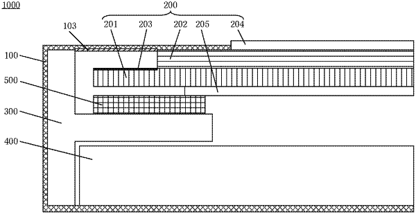
1. A tape, comprising:
a substrate;
a conductive adhesive layer disposed on the substrate; and
an insulating layer disposed on a part of a bonding surface of the conductive adhesive layer, wherein the insulating layer is configured to insulate the conductive adhesive layer from a conducting part of an object to be bonded;
wherein the insulating layer has a multi-layer structure, and the insulating layer includes: at least one insulating resin layer stacked along a direction of the conductive adhesive layer facing away from the substrate, and an insulating adhesive layer located on a surface of the at least one insulating resin layer facing away from the substrate;
wherein an orthographic projection of the insulating layer on the substrate is within an orthographic projection of the conductive adhesive layer on the substrate, and at least a part of an outer contour of the orthographic projection of the insulating layer on the substrate and an outer contour of the orthographic projection of the conductive adhesive layer on the substrate have a space therebetween, wherein the insulating layer is disposed in a central region of the conductive adhesive layer, and there is the space between all edges of the insulating layer and corresponding edges of the conductive adhesive layer;
wherein the substrate is a light-shielding substrate, and the substrate is made of a material that is opaque or has a light transmittance less than or equal to 10%; or
the conductive adhesive layer is a light-shielding conductive adhesive layer, and the conductive adhesive layer is made of conductive glue that is opaque or has a light transmittance less than or equal to 10%.
|