| CPC B23K 26/362 (2013.01) [B23K 26/0643 (2013.01); B23K 26/0648 (2013.01); B23K 2103/50 (2018.08)] | 8 Claims |
|
1. A process of producing optical devices, comprising:
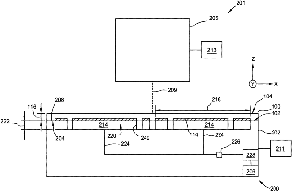
transferring a first substrate comprising a plurality of optical devices to a laser dicing tool, each optical device of the plurality of optical devices having a contour surrounding regions of device structures, the laser dicing tool comprising a filamentation stage and a singulation stage;
dicing the plurality of optical devices, each optical device is diced along the contour surrounding regions of the device structures, the first substrate is disposed in the filamentation stage with projections of the filamentation stage contacting portions of the plurality of optical devices between the regions of device structures;
separating the plurality of optical devices, each optical device is separated along the surrounding regions of the device structures, the first substrate disposed in the singulation stage with projections of the singulation stage contacting portions of the plurality of optical devices between the regions of device structures; and
transferring the devices to a backend storage port or to a backend processor.
|