| CPC B01L 3/50273 (2013.01) [C12M 23/16 (2013.01); C12M 29/10 (2013.01); B01L 2200/0647 (2013.01); B01L 2200/12 (2013.01); B01L 2300/0816 (2013.01); B01L 2300/0887 (2013.01); B01L 2300/12 (2013.01); B01L 2300/161 (2013.01); B01L 2400/0427 (2013.01)] | 27 Claims |
|
1. A method of manufacturing a microfluidic apparatus, the method comprising:
bonding a spacing element to an inner surface of a cover having at least one electrode configured to be connected to a voltage source;
bonding the spacing element and cover to a dielectric surface of a substrate having at least one electrode configured to be connected to a voltage source, whereby the spacing element becomes sandwiched between the inner surface of the cover and the dielectric surface of the substrate, with the cover and the substrate oriented substantially parallel to one another, and the substrate, spacing element, and cover collectively defining an enclosure configured to hold a liquid;
forming, by vapor deposition, a densely packed hydrophobic monolayer on at least a portion of the inner surface of the cover, wherein the hydrophobic monolayer comprises self-associating molecules covalently bonded to the inner surface of the cover; and
forming, by vapor deposition, a densely packed hydrophobic monolayer on at least a portion of the dielectric surface of the substrate, wherein the hydrophobic monolayer comprises self-associating molecules covalently bonded to the dielectric surface of the substrate
wherein the self-associating molecules of the hydrophobic monolayer of the cover and the self-associating molecules of the hydrophobic monolayer of the substrate each comprise a surface modifying ligand and a linking group that links the surface modifying ligand to the inner surface of the cover and the dielectric surface of the substrate, respectively, wherein the resulting surfaces of the cover and the substrate have a structure of Formula II:
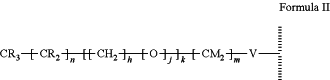 wherein
 is a surface of the dielectric layer; is a surface of the dielectric layer;V is —P(O)(OY)W— or —Si(OZ)2W—;
W is —O—, —S—, or —NH— and connects to the surface;
Z is a bond to an adjacent silicon atom attached to the surface or is a bond to the surface;
Y is a bond to an adjacent phosphorus atom attached to the surface or is a bond to the surface;
R is hydrogen or fluorine;
M is hydrogen or fluorine;
h is independently an integer of 2 or 3;
j is 1;
k is 0 or 1;
m is 0 or an integer of 1 to 20
n is 0 or an integer of 1 to 20;
the sum of (n+[(h+j)·k]+m) is an integer of 11 to 25;
when k is 1, then m is at least 2 and M is hydrogen; and
when k is 0 and R is fluorine, then m is at least 2 and M is hydrogen.
|