| CPC H10K 59/65 (2023.02) [G09F 9/30 (2013.01); H04N 5/33 (2013.01); H04N 23/54 (2023.01); G02F 1/1333 (2013.01); G02F 2201/083 (2013.01); G02F 2201/58 (2013.01)] | 16 Claims |
|
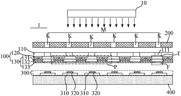
1. A display panel, comprising:
a display layer configured to display an image, the display layer having light-transmitting portions, and the light-transmitting portions being configured to transmit infrared light;
a photosensitive layer disposed on a side of the display layer; and
an infrared mask disposed on a side of the photosensitive layer proximate to the display layer, the infrared mask having hollowed-out regions configured to make the infrared mask have a preset pattern, and a region in the infrared mask except the hollowed-out regions being configured to prevent transmission of infrared light; the photosensitive layer being configured to receive infrared light passing through the hollowed-out regions and the light-transmitting portions, and convert the infrared light into an image signal;
wherein the display layer includes a driving circuit layer and a light-emitting layer that are stacked, the light-emitting layer includes a plurality of pixel units, and the driving circuit layer is coupled to the plurality of pixel units and is configured to drive the plurality of pixel units to emit light.
|