| CPC H10K 59/131 (2023.02) [G09G 3/3233 (2013.01); G09G 2300/0413 (2013.01); G09G 2300/0426 (2013.01); G09G 2300/0819 (2013.01); G09G 2300/0842 (2013.01); G09G 2320/0233 (2013.01); H01L 27/124 (2013.01); H10K 59/1213 (2023.02); H10K 59/351 (2023.02); H10K 59/352 (2023.02); H10K 59/88 (2023.02)] | 20 Claims |
|
1. A display substrate, comprising:
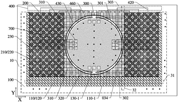
a base substrate, comprising a first display region and a second display region, wherein the first display region comprises a plurality of first light emitting unit groups and a plurality of first pixel circuit groups respectively connected with the plurality of first light emitting unit groups; the second display region comprises a plurality of second light emitting unit groups and a plurality of second pixel circuit groups respectively connected with the plurality of second light emitting unit groups; a density of the plurality of second light emitting unit groups is smaller than a density of the plurality of first light emitting unit groups; each light emitting unit group comprises a plurality of light emitting units, and each of the light emitting units comprises a first electrode, a light emitting layer and a second electrode which are arranged in a direction perpendicular to the base substrate, and the second electrode is located at a side of the light emitting layer facing the base substrate;
a plurality of reset power signal lines, located between the second electrodes of the light emitting units and the base substrate; and
a plurality of data lines, located at a side of the plurality of reset power signal lines away from the base substrate, and an extending direction of the plurality of data lines intersecting with an extending direction of the plurality of reset power signal lines;
wherein each pixel circuit group comprises a plurality of pixel circuits, the plurality of second pixel circuit groups comprise a plurality of first pixel circuit units, each first pixel circuit unit at least comprises a first pixel circuit and a second pixel circuit, and at least two pixel circuits in the first pixel circuit unit are configured to be electrically connected with the second electrode of a same light emitting unit,
each of the plurality of pixel circuits comprises a data writing transistor, a driving transistor and a first reset transistor, a first electrode of the first reset transistor is connected with one of the plurality of reset power signal lines, a second electrode of the first reset transistor is connected with the second electrode of a corresponding light emitting unit, and a first electrode of the data writing transistor is connected with a second electrode of the driving transistor,
the display substrate further comprises a plurality of first connection portions, a first end of each first connection portion of at least part of the first connection portions is connected with a second electrode of the data writing transistor of the first pixel circuit, and a second end of each first connection portion of the at least part of the first connection portions is connected with a second electrode of the data writing transistor of the second pixel circuit to connect at least two data writing transistors of the first pixel circuit unit with a same data line, at least portion of each first connection portion of the at least part of the first connection portions is located between the second electrode of the data writing transistor and the first electrode of the first reset transistor in the first pixel circuit.
|