| CPC H10K 59/131 (2023.02) [G09G 3/3233 (2013.01); H10K 50/813 (2023.02); H10K 71/00 (2023.02); G09G 2300/0426 (2013.01); G09G 2300/0842 (2013.01); G09G 2310/08 (2013.01); H10K 59/1201 (2023.02); H10K 59/351 (2023.02)] | 20 Claims |
|
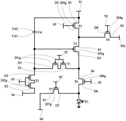
1. A display substrate, comprising a base and a plurality of subpixels distributed in an array on the base, wherein the plurality of subpixels comprise a first subpixel and a second subpixel, each of the subpixels comprises:
a power signal line pattern, wherein the power signal line pattern comprises a first power line portion and a second power line portion; and at least a part of the first power line portion extends in a first direction; and
a light-emitting element, wherein the light-emitting element comprises an anode pattern;
and in the display substrate,
an overlap between the anode pattern of the first subpixel and the power signal line pattern is larger in area than an overlap between the anode pattern of the second subpixel and the power signal line pattern, and
an overlap between the anode pattern of the first subpixel and the first power line portion is larger in area than an overlap between the anode pattern of the first subpixel and the second power line portion.
|