| CPC H05K 3/462 (2013.01) [G01R 3/00 (2013.01); H01R 12/523 (2013.01); H05K 3/0032 (2013.01); H05K 3/4069 (2013.01); H05K 3/4638 (2013.01); H05K 2203/068 (2013.01); H05K 2203/1131 (2013.01)] | 13 Claims |
|
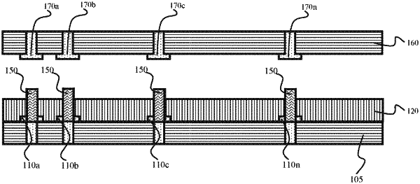
1. A method for attaching a testing PCB to a space transformer, comprising:
fabricating a testing PCB;
fabricating a space transformer; and
prior to attaching a component to the testing PCB that would be damaged by a lamination press;
securing resin prepreg to an attachment side of the testing PCB;
fabricating a hole through the resign prepreg at a location of an electrical connection on the testing PCB;
filling the hole with sintering paste;
pressure treating the testing PCB (along with the resin prepreg and sintering paste);
using a lamination press cycle to attach an attachment side of the space transformer to the side of the resin prepreg opposite the testing PCB such that an electrical connection on the space transformer is aligned with the sintering paste in the hole.
|