| CPC H01L 29/7869 (2013.01) [H01L 21/02565 (2013.01); H01L 21/02667 (2013.01); H01L 27/1207 (2013.01); H01L 27/1225 (2013.01); H01L 27/124 (2013.01); H01L 27/1255 (2013.01); H01L 29/24 (2013.01); H01L 29/66969 (2013.01); H01L 29/78648 (2013.01); H01L 29/78696 (2013.01); H10B 99/00 (2023.02)] | 20 Claims |
|
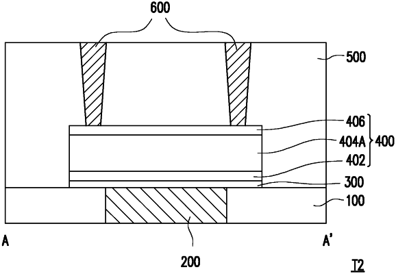
1. A transistor, comprising:
a first gate electrode;
a first capping layer, a crystalline semiconductor oxide layer, and a second capping layer sequentially disposed over the first gate electrode, wherein sidewalls of the second capping layer are aligned along a line perpendicular to a top surface of the first gate electrode with sidewalls of the crystalline semiconductor oxide layer;
a first gate dielectric layer located between the first gate electrode and the first capping layer; and
source/drain contacts disposed on the second capping layer, wherein the crystalline semiconductor oxide layer and the source/drain contacts are located on two opposite sides of the second capping layer.
|