| CPC H01L 29/7851 (2013.01) [H01L 21/823418 (2013.01); H01L 21/823431 (2013.01); H01L 29/267 (2013.01); H01L 29/41791 (2013.01); H01L 29/66795 (2013.01)] | 20 Claims |
|
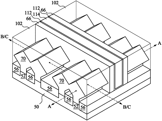
1. A structure comprising:
a semiconductor substrate having a channel region;
a gate stack over the channel region; and
an epitaxial source/drain region adjacent the gate stack, the epitaxial source/drain region comprising:
a main portion in the semiconductor substrate, the main portion comprising a semiconductor material doped with gallium, a first concentration of gallium in the main portion being less than the solid solubility of gallium in the semiconductor material; and
a finishing portion over the main portion, the finishing portion doped with gallium, a second concentration of gallium in the finishing portion being greater than the solid solubility of gallium in the semiconductor material, the second concentration being greater than the first concentration.
|