| CPC H01L 21/4857 (2013.01) [H01L 21/6835 (2013.01); H01L 23/49822 (2013.01); H01L 23/5389 (2013.01); H01L 24/92 (2013.01); H01L 21/4853 (2013.01); H01L 21/56 (2013.01); H01L 21/561 (2013.01); H01L 21/568 (2013.01); H01L 23/3128 (2013.01); H01L 23/49816 (2013.01); H01L 24/11 (2013.01); H01L 24/13 (2013.01); H01L 24/16 (2013.01); H01L 24/32 (2013.01); H01L 24/81 (2013.01); H01L 24/83 (2013.01); H01L 24/97 (2013.01); H01L 2221/68304 (2013.01); H01L 2221/68318 (2013.01); H01L 2221/68331 (2013.01); H01L 2221/68345 (2013.01); H01L 2221/68363 (2013.01); H01L 2224/1132 (2013.01); H01L 2224/131 (2013.01); H01L 2224/13294 (2013.01); H01L 2224/133 (2013.01); H01L 2224/16227 (2013.01); H01L 2224/16237 (2013.01); H01L 2224/16238 (2013.01); H01L 2224/32225 (2013.01); H01L 2224/73204 (2013.01); H01L 2224/81005 (2013.01); H01L 2224/81192 (2013.01); H01L 2224/81203 (2013.01); H01L 2224/81224 (2013.01); H01L 2224/81424 (2013.01); H01L 2224/81439 (2013.01); H01L 2224/81444 (2013.01); H01L 2224/81447 (2013.01); H01L 2224/81464 (2013.01); H01L 2224/81815 (2013.01); H01L 2224/8191 (2013.01); H01L 2224/81911 (2013.01); H01L 2224/81913 (2013.01); H01L 2224/81914 (2013.01); H01L 2224/83 (2013.01); H01L 2224/83005 (2013.01); H01L 2224/83104 (2013.01); H01L 2224/83192 (2013.01); H01L 2224/92 (2013.01); H01L 2224/9202 (2013.01); H01L 2224/92125 (2013.01); H01L 2224/97 (2013.01); H01L 2924/1421 (2013.01); H01L 2924/1433 (2013.01); H01L 2924/14335 (2013.01); H01L 2924/15311 (2013.01); H01L 2924/15331 (2013.01); H01L 2924/1815 (2013.01); H01L 2924/18161 (2013.01)] | 18 Claims |
|
1. A method of manufacturing a semiconductor device, the method comprising:
forming, on a carrier top side of a carrier, layers of an upper signal distribution structure;
coupling a bottom side of a semiconductor component to a top side of the upper signal distribution structure; and
after coupling the semiconductor component, forming, on a bottom side of the upper signal distribution structure, layers of a lower signal distribution structure;
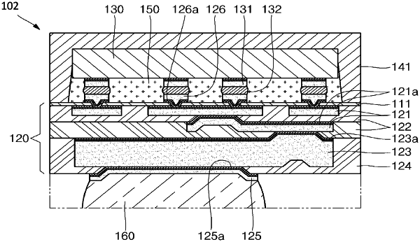
wherein the layers of the lower signal distribution structure include a first dielectric layer and a first conductive layer;
wherein the first conductive layer of the lower signal distribution structure extends into a first opening in the first dielectric layer of the lower signal distribution structure and towards the upper signal distribution structures;
wherein the lower signal distribution structure comprises an under bump metal structure that has a concave shape that opens downward;
wherein the under bump metal structure comprises a bump upper side and a bump lower side; and
wherein the bump upper side is coupled to a bottom side of the lower signal distribution structure.
|