| CPC H01L 21/30612 (2013.01) [H01L 21/308 (2013.01); H01L 22/26 (2013.01); H01L 29/2003 (2013.01); H01L 29/66522 (2013.01); H01L 29/66666 (2013.01); H01L 29/7827 (2013.01)] | 18 Claims |
|
1. A field-effect transistor (FET) device, comprising:
a semiconductor substrate;
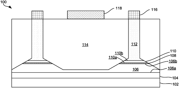
a first semiconductor layer coupled to the semiconductor substrate, wherein the first semiconductor layer is characterized by a first conductivity type and a first dopant concentration;
a second semiconductor layer coupled to the first semiconductor layer, wherein the second semiconductor layer is characterized by the first conductivity type;
a marker layer coupled to the second semiconductor layer;
a third semiconductor layer coupled to the marker layer, wherein the third semiconductor layer is characterized by the first conductivity type;
a plurality of fins coupled to the third semiconductor layer, wherein each of the plurality of fins is separated by one of a plurality of recess regions extending to the second semiconductor layer, wherein the each of the plurality of fins is characterized by the first conductivity type and a second dopant concentration;
a fifth semiconductor layer epitaxially grown within the plurality of recess regions, wherein the fifth semiconductor layer is characterized by a second conductivity type opposite to the first conductivity type;
a source metal layer coupled to each of the plurality of fins; and
a gate metal layer coupled to the fifth semiconductor layer.
|