| CPC G09G 3/3233 (2013.01) [G09G 2300/0842 (2013.01); G09G 2310/061 (2013.01); G09G 2320/0233 (2013.01)] | 19 Claims |
|
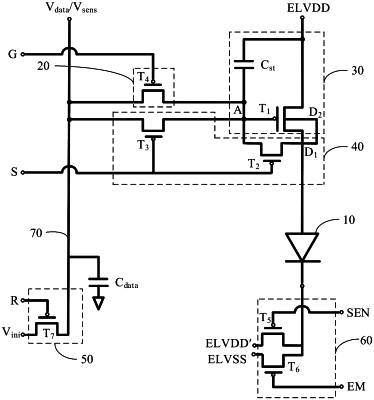
1. A pixel circuitry, comprising a driving circuit, a first switching circuit, a second switching circuit and a light-emitting element,
wherein the driving circuit is configured to, under a control of a voltage transferred by the first switching circuit, drive the light-emitting element to emit light, and the driving circuit comprises a first transistor and a storage capacitor;
the first transistor is a four-end transistor comprising a first end, a second end, a third end and a control end; the control end of the first transistor is electrically connected to the first switching circuit, the first end of the first transistor is electrically connected to a first voltage end, the second end of the first transistor is electrically connected to an anode of the light-emitting element, and the third end of the first transistor is electrically connected to the second switching circuit;
a first end of the storage capacitor is electrically connected to the first voltage end, and a second end of the storage capacitor is electrically connected to the control end of the first transistor;
the first switching circuit is electrically connected to a data sensing line, and configured to write a voltage on the data sensing line into the storage capacitor in an on state in response to a first scanning signal from a first scanning line;
the second switching circuit is electrically connected to the data sensing line, and configured to enable the third end of the first transistor to be electrically connected to the data sensing line in the on state in response to a second scanning signal from a second scanning line;
wherein the pixel circuitry further comprises a resetting circuit, the data sensing line is electrically connected to the resetting circuit, the resetting circuit is configured to reset a potential at the data sensing line to an initialization voltage in response to a resetting signal, and a secondary driving transistor is configured to be turned on under a control of the initialization voltage.
|