| CPC G09G 3/32 (2013.01) [G09G 2300/0426 (2013.01); G09G 2310/0267 (2013.01); G09G 2310/0286 (2013.01)] | 20 Claims |
|
1. A display substrate, comprising:
a base substrate, comprising a display region and a peripheral region on at least one side of the display region; and
a first gate driving circuit and a plurality of signal lines electrically connected to the first gate driving circuit in the peripheral region of the base substrate,
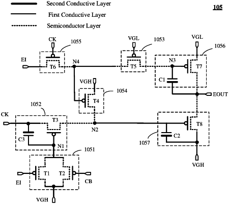
wherein the first gate driving circuit comprises a plurality of cascaded shift register units, and the plurality of signal lines are configured to respectively provide a trigger signal, at least one clock signal, and at least one power signal to the cascaded shift register units;
each of the plurality of signal lines comprises a first conductive portion;
for at least one signal line in the plurality of signal lines, the display substrate comprises a multi-layer insulating pattern on a side of the first conductive portion of each signal line away from the base substrate, and at least one insulating pattern in the multi-layer insulating pattern covers a surface of a side of the first conductive portion away from the base substrate;
the multi-layer insulating pattern comprises at least one first insulating pattern, the first insulating pattern comprises at least one hollow, and an orthographic projection of the at least one hollow on the base substrate is at least partially in a region surrounded by an orthographic projection of the first conductive portion on the base substrate;
a material of the first insulating pattern comprises an organic insulating material; and
for the at least one signal line, each signal line further comprises a second conductive portion,
the second conductive portion is on a side of the first conductive portion away from the base substrate and is configured to be electrically connected to the first conductive portion, and
at least one insulating pattern in the multi-layer insulating pattern covers a surface of a side of the second conductive portion away from the base substrate.
|