| CPC G06F 3/0613 (2013.01) [G06F 3/0611 (2013.01); G06F 3/0631 (2013.01); G06F 3/0659 (2013.01); G06F 3/067 (2013.01)] | 20 Claims |
|
1. A system comprising:
a processing circuitry having a device coupled with one or more external memory devices, the device to:
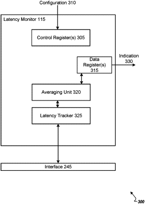
identify a configuration stored within a control register of the device, wherein the configuration indicates an external memory device of the one or more external memory devices;
detect, by a hardware latency tracker of the device coupled with an interface to the external memory device of the one or more external memory devices, an input/output (IO) request associated with the external memory device;
responsive to detecting the IO request associated with the external memory device, store a first timestamp in a data register;
detect, by the hardware latency tracker, an indication from the external memory device of a completion of the IO request associated with the external memory device;
responsive to detecting the indication, store a second timestamp in the data register; and
determine, by an averaging unit of the device, a latency associated with the IO request using the first timestamp and the second timestamp.
|