| CPC G01R 19/165 (2013.01) [H03F 3/04 (2013.01); H03K 5/24 (2013.01)] | 10 Claims |
|
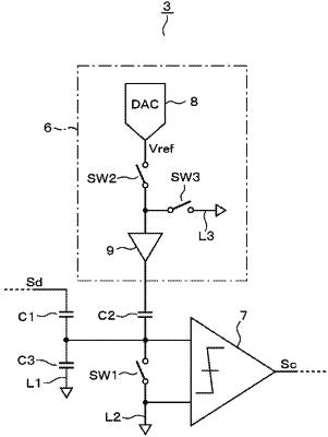
1. A signal detection circuit that detects, as a detection target signal, a signal of a main terminal of a switching element by comparing the detection target signal with a reference signal, the signal detection circuit comprising:
a signal generation unit generating the reference signal;
a first capacitor having a first terminal connected with the main terminal of the switching element;
a second capacitor having a first terminal connected with an output terminal of the signal generation unit; and
a detection circuit receiving, as input signals, a signal output from a second terminal of the first capacitor and a signal output from a second terminal of the second capacitor, and the detection circuit detecting the detection target signal based on the input signals.
|