| CPC B23K 26/38 (2013.01) [B28D 5/0011 (2013.01); G01N 21/9505 (2013.01); B23K 2103/50 (2018.08); H01L 29/1608 (2013.01)] | 12 Claims |
|
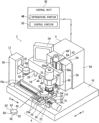
1. A SiC wafer manufacturing method for manufacturing a SiC wafer from a SiC ingot having an end surface, the SiC wafer manufacturing method comprising the steps of:
verifying a condition of test cracks comprising applying a test laser beam to the SiC ingot in a predetermined area in a condition where the focal point of the test laser beam is set inside the SiC ingot at a predetermined depth from the end surface of the SiC ingot, the predetermined depth corresponding to the thickness of the SiC wafer to be manufactured, the test laser beam having a transmission wavelength transmissible through SiC, thereby forming a test separation layer inside the SiC ingot at the predetermined depth, the test separation layer having a first test modified portion at the predetermined depth where SiC is separated into Si and C and first test cracks extending from the first test modified portion along a c-plane in the SiC ingot;
providing relative movement between the SiC ingot and the test laser beam in a direction perpendicular to a length of the first test modified portion and forming a second test modified portion parallel to the first test modified portion and aligned therewith, thereby forming the second test modified portion inside the SiC ingot at the predetermined depth, the second test modified portion where SiC is separated into Si and C, wherein second test cracks from the second test modified portion along a c-plane in the SiC ingot;
forming a separation layer by applying a laser beam to the SiC ingot in a condition where the focal point of the laser beam is set inside the SiC ingot at the predetermined depth from the end surface of the SiC ingot after performing the verifying step, the predetermined depth corresponding to the thickness of the SiC wafer to be manufactured, the laser beam having a transmission wavelength transmissible through SiC, thereby forming the separation layer inside the SiC ingot at the predetermined depth, the separation layer inside the SiC ingot having a modified portion where SiC is separated into Si and C and cracks extending from the modified portion along the c-plane in the SiC ingot; and
separating the SiC wafer from the SiC ingot along the separation layer after performing the separation layer forming step,
the verifying step including setting the power of the test laser beam to a power at which the first and second test cracks are formed, such that the first and second test cracks overlap in the direction perpendicular to the length of the first test modified portion and in which the verifying step confirms whether or not the first and second test cracks have been formed, such that the first and second test cracks overlap in the direction perpendicular to the length of the first test modified layer.
|