| CPC G02F 1/133528 (2013.01) [G02B 5/3058 (2013.01); G02B 27/283 (2013.01); G02F 1/133548 (2021.01); G02F 1/292 (2013.01)] | 9 Claims |
|
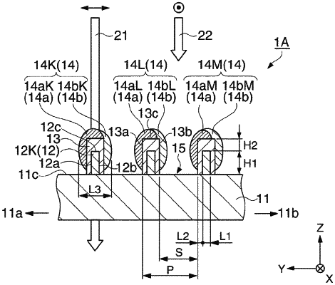
[ 22. A polarization device comprising:
a substrate;
a first metal layer that is provided at a first surface of the substrate, the first metal layer having a stripe shape;
a second metal layer that is provided adjacent to the first metal layer at the first surface of the substrate, the second metal layer having a stripe shape;
a groove that is provided between the first metal layer and the second metal layer] [ , the groove having a bottom surface in the substrate] [ ;
a first dielectric layer that is provided at a first side part of the first metal layer, a second side part of the first metal layer facing the first side part and a top part of the first metal layer; and
a second dielectric layer that is provided on the first dielectric layer,
wherein an optical absorption rate of the second dielectric layer is higher than that of the first dielectric layer,
wherein a substrate side first end portion of the second dielectric layer is located at a first side part of the first dielectric layer between the first surface of the substrate] [ , which is the bottom surface of the groove, ] [ and the top part of the first metal layer,
wherein a substrate side second end portion of the second dielectric layer is located at a second side part of the first dielectric layer between the first surface of the substrate] [ , which is the bottom surface of the groove, ] [ and the top part of the first metal layer,
wherein a substrate side first end portion of the first dielectric layer is located at a first side part of the first metal layer between the first surface of the substrate] [ , which is the bottom surface of the groove, ] [ and the substrate side first end portion of the second dielectric layer, and
wherein a substrate side second end portion of the first dielectric layer is located at a second side part of the first metal layer between the first surface of the substrate] [ , which is the bottom surface of the groove, ] [ and the substrate side second end portion of the second dielectric layer.]
|