| CPC H10N 70/841 (2023.02) [H10B 63/00 (2023.02); H10B 63/30 (2023.02); H10N 70/011 (2023.02); H10N 70/063 (2023.02); H10N 70/066 (2023.02); H10N 70/24 (2023.02); H10N 70/801 (2023.02); H10N 70/826 (2023.02); H10N 70/8833 (2023.02)] | 20 Claims |
|
1. An integrated circuit (IC), comprising:
a semiconductor substrate including a memory region and a logic region;
an interconnect structure disposed over the memory region and the logic region, the interconnect structure including a first lower metal line and a first upper metal line disposed over the memory region and isolated from one another by an interlayer dielectric material, and a second lower metal line and a second upper metal line disposed over the logic region and isolated from one another by the interlayer dielectric material;
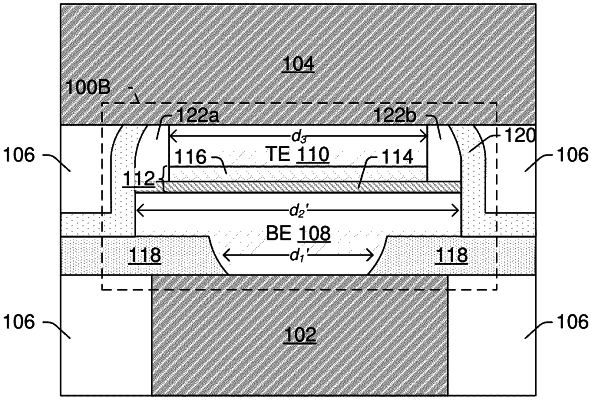
a memory cell or metal-insulator-metal (MIM) capacitor disposed over the memory region and spanning a first vertical distance that separates an upper surface of the first lower metal line from a lower surface of the first upper metal line, the memory cell or MIM capacitor including:
a bottom electrode disposed over the memory region and coupled to an upper portion of the first lower metal line;
a data storage or dielectric layer disposed over the bottom electrode; and
a top electrode disposed over the data storage or dielectric layer and coupled to a lower portion of the first lower metal line, wherein the data storage or dielectric layer separates the bottom electrode from the top electrode, and wherein the top electrode has an upper planar surface which extends continuously between sidewalls of the top electrode and which directly abuts a corresponding co-planar surface of the first upper metal line; and
a logic interconnect structure disposed over the logic region and spanning a second vertical distance that separates an upper surface of the second lower metal line from a lower surface of the second upper metal line, the second vertical distance being equal to the first vertical distance, the logic interconnect structure including:
a via disposed over the logic region and spanning an entirety of the second vertical distance.
|