| CPC H10N 70/231 (2023.02) [H10B 63/30 (2023.02); H10N 70/021 (2023.02); H10N 70/061 (2023.02); H10N 70/841 (2023.02); H10N 70/8825 (2023.02); H10N 70/8828 (2023.02)] | 20 Claims |
|
1. A memory device, comprising:
a substrate;
a transistor disposed over the substrate;
an interconnect structure disposed over and electrically connected to the transistor; and
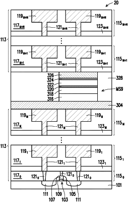
a memory stack disposed between two adjacent metallization layers of the interconnect structure and comprising:
a bottom electrode disposed over the substrate and electrically connected to a bit line;
a memory layer disposed over the bottom electrode;
a selector layer disposed over the memory layer; and
a top electrode disposed over the selector layer and electrically connected to a word line,
wherein at least one moisture-resistant layer is provided adjacent to and in contact with the selector layer, the at least one moisture-resistant layer comprises an amorphous material.
|