US 11,944,017 B2
Semiconductor structure and manufacturing method of the same
Tai-Yen Peng, Hsinchu (TW); Yu-Shu Chen, Hsinchu (TW); Chien Chung Huang, Taichung (TW); Sin-Yi Yang, Taichung (TW); Chen-Jung Wang, Hsinchu (TW); Han-Ting Lin, Hsinchu (TW); Jyu-Horng Shieh, Hsin-Chu (TW); and Qiang Fu, Hsinchu (TW)
Assigned to TAIWAN SEMICONDUCTOR MANUFACTURING COMPANY LTD., Hsinchu (TW)
Filed by TAIWAN SEMICONDUCTOR MANUFACTURING COMPANY LTD., Hsinchu (TW)
Filed on May 5, 2023, as Appl. No. 18/312,723.
Application 17/103,577 is a division of application No. 16/242,689, filed on Jan. 8, 2019, granted, now 10,862,023, issued on Dec. 8, 2020.
Application 18/312,723 is a continuation of application No. 17/103,577, filed on Nov. 24, 2020, granted, now 11,683,991.
Claims priority of provisional application 62/711,803, filed on Jul. 30, 2018.
Prior Publication US 2023/0276715 A1, Aug. 31, 2023
Int. Cl. H10N 50/80 (2023.01); H10N 50/01 (2023.01); H10N 50/85 (2023.01)
CPC H10N 50/80 (2023.02) [H10N 50/01 (2023.02); H10N 50/85 (2023.02)] 20 Claims
OG exemplary drawing
 
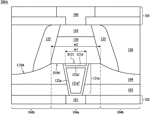
1. A semiconductor structure, comprising:
an insulation layer;
a bottom electrode via in the insulation layer, comprising a conductive portion and a capping layer over the conductive portion;
a barrier layer surrounding the bottom electrode via; and
a magnetic tunneling junction (MTJ) over the bottom electrode via.