| CPC H10N 50/10 (2023.02) [G11C 11/161 (2013.01); H10B 61/22 (2023.02); H10N 50/80 (2023.02); H10N 50/85 (2023.02)] | 20 Claims |
|
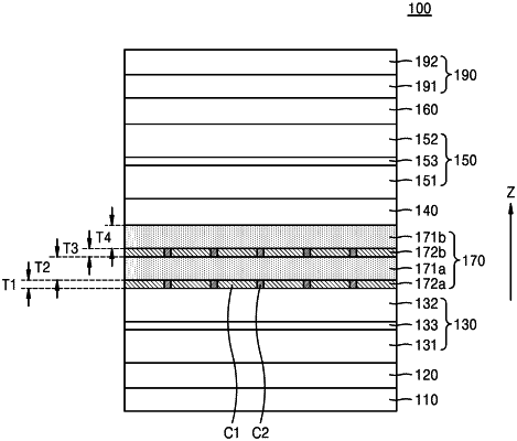
1. A magnetic memory device comprising a magnetic tunnel junction, wherein the magnetic tunnel junction comprises:
a fixed layer;
a polarization enhancement structure on the fixed layer;
a tunnel barrier layer on the polarization enhancement structure; and
a free layer on the tunnel barrier layer,
wherein the polarization enhancement structure comprises a plurality of polarization enhancement layers and at least one spacer layer which separates the plurality of polarization enhancement layers from each other, with a first and second of the plurality of polarization enhancement layers both directly contacting a spacer layer of the at least one spacer layer therebetween,
wherein each of the plurality of polarization enhancement layers comprises a ferromagnetic material and each of at least one spacer layers comprises a ferromagnetic material and a non-magnetic material,
wherein a thickness of each of the plurality of polarization enhancement layers is from about 5 Å to about 20 Å, and
wherein a thickness of the at least one spacer layer is from about 2 Å to about 15 Å.
|