| CPC H10N 50/01 (2023.02) [G11C 11/161 (2013.01); H01L 21/76802 (2013.01); H01L 21/76883 (2013.01); H01L 23/5226 (2013.01); H10B 61/00 (2023.02); H10N 50/10 (2023.02); H10N 50/80 (2023.02); H10N 50/85 (2023.02)] | 9 Claims |
|
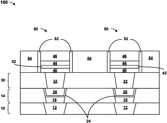
1. A semiconductor device comprising:
a via dielectric layer sandwiched between a metal line layer and a bottom electrode of a magnetic tunnel junction (MTJ) stack;
a via in the via dielectric layer, wherein the via comprises an upper metal stud and a lower metal stud, wherein the upper metal stud and the lower metal stud each comprise cobalt;
a liner surrounding a lower horizontal surface and vertical side surfaces of the upper metal stud, wherein the liner is sandwiched between the upper metal stud and the lower metal stud, wherein the liner comprises a non-ferromagnetic conductive material, wherein a thickness of the liner corresponds to a least amount of influence of a magnetic field through the non-ferromagnetic conductive material of the liner between the upper metal stud and the lower metal stud.
|