| CPC H10N 10/01 (2023.02) [C04B 35/117 (2013.01); C04B 35/488 (2013.01); C04B 35/6261 (2013.01); C04B 35/62813 (2013.01); C04B 35/62823 (2013.01); C04B 35/62884 (2013.01); C04B 35/64 (2013.01); C09C 1/28 (2013.01); C09C 3/006 (2013.01); C09C 3/041 (2013.01); C09C 3/043 (2013.01); C09C 3/063 (2013.01); H10N 10/852 (2023.02); H10N 10/857 (2023.02); C01P 2002/60 (2013.01); C01P 2002/88 (2013.01); C01P 2004/64 (2013.01); C01P 2006/32 (2013.01); C01P 2006/40 (2013.01); C04B 2235/3217 (2013.01); C04B 2235/3244 (2013.01); C04B 2235/428 (2013.01); C04B 2235/5445 (2013.01); C04B 2235/5454 (2013.01); C04B 2235/614 (2013.01); C04B 2235/781 (2013.01); C04B 2235/785 (2013.01); C04B 2235/9607 (2013.01)] | 20 Claims |
|
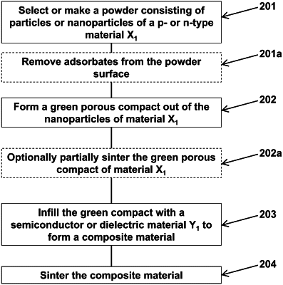
1. A method for forming a thermoelectric (TE) nanocomposite material, the method including steps of:
making or selecting a first material comprising a nanopowder of n- or p-type semiconductor nanoparticles or of X1/X2 . . . XN n˜ or p˜type semiconductor core/shell nanoparticles, where X1 is a core of the nanoparticles and X2/ . . . XN are shells surrounding the core wherein, —X2 . . .XN-1 are intermediate continuous or discontinuous layers, each shell surrounding a shell preceding it, and XN is an outer continuous or discontinuous shell;
making a porous green compact consisting of an interconnected particle network from the first material, the compact having an open porosity allowing permeation of the compact with gas or liquid;
infilling and coating all available surfaces inside the porous compact formed from the first material with at least one second material Y1, Y2, . . . YN to form a composite material of the first and second materials, at least one second material Y1, Y2, . . . YN being a semiconductor or a dielectric/insulator material and having a thermal conductivity lower than a thermal conductivity of the first material; and
sintering the formed nanocomposite material to remove residual porosity from the composite material and form a nanocomposite solid material with intimately connected p- or n-type networks and having strong chemical bonds at all interfaces;
wherein the nanocomposite solid material retains the nanostructure of the starting nanoparticles within the solid;
wherein the nanocomposite solid material maintains a percolating p- or n-type semiconductor network of the first material X1/X2 . . . XN within the solid second material; and
wherein the second material provides efficient phonon scattering so as to reduce a thermal conductivity of the nanocomposite material while maintaining electrical transport properties of the first material network.
|