| CPC H10K 77/111 (2023.02) [C23C 14/18 (2013.01); C23C 16/345 (2013.01); C23C 16/401 (2013.01); C23C 28/30 (2013.01); H10K 50/844 (2023.02); H10K 59/12 (2023.02); H10K 71/00 (2023.02); H10K 71/80 (2023.02); G09G 3/3233 (2013.01); G09G 2300/0443 (2013.01); G09G 2300/0809 (2013.01); H10K 59/1201 (2023.02)] | 15 Claims |
|
1. A display device, comprising:
a first base substrate;
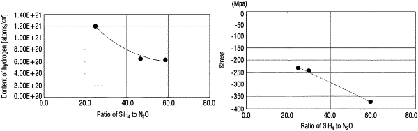
a first barrier layer disposed on the first base substrate and including a silicon oxide having a hydrogen content between 1.20E+21 and 1.60E+21 atoms/cm3;
a second base substrate disposed on the first barrier layer;
at least one transistor disposed on the second base substrate; and
an organic light emitting diode disposed on the at least one transistor,
wherein the first barrier layer is disposed between the first base substrate and second base substrate,
wherein an adhesion force between the first barrier layer and the second base substrate is between 200 gf/inch and 330 gf/inch, and SiO bonding peak of the first barrier layer is between 1045 and 1049 nm.
|