| CPC H10K 59/1315 (2023.02) [H10K 59/1201 (2023.02)] | 16 Claims |
|
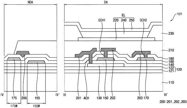
1. A display device including a display area and a non-display area surrounding at least a portion of the display area, the display device comprising:
a base substrate;
a buffer layer disposed on the base substrate;
an active layer disposed on the buffer layer in the display area;
a first gate insulation layer disposed on the active layer;
a first gate line disposed on the first gate insulation layer in the display area;
a first signal line disposed in a same layer as the first gate line in the non-display area, the first signal line including a same material as a material of the first gate line including molybdenum;
a second gate insulation layer disposed on the first gate line and the first signal line;
a second gate line disposed on the second gate insulation layer in the display area; and
a second signal line disposed in a same layer as the second gate line in the non-display area, the second signal line including a same material as a material of the second gate line including at least one of aluminum and an aluminum alloy,
wherein a width of the first signal line is greater than a width of the second signal line.
|