| CPC H10K 59/131 (2023.02) [G09G 3/3233 (2013.01); G09G 3/3266 (2013.01); G09G 2300/0426 (2013.01); G09G 2300/0819 (2013.01); G09G 2300/0852 (2013.01); G09G 2310/0297 (2013.01); G09G 2330/12 (2013.01)] | 19 Claims |
|
1. A display substrate, comprising:
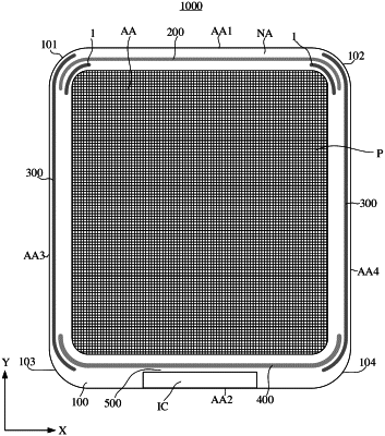
a base substrate, comprising a display area and a bezel area located on at least one side of the display area;
a plurality of pixel units located in the display area and arranged in an array along a row direction and a column direction on the base substrate, wherein each pixel unit comprises a plurality of sub-pixels;
a plurality of scanning signal lines disposed on the base substrate, wherein the plurality of scanning signal lines are configured to provide a scanning signal to a plurality of rows of sub-pixels respectively;
a gate driver circuit disposed on the base substrate and located in the bezel area, wherein the gate driver circuit is configured to output the scanning signal;
a plurality of load compensation units disposed on the base substrate and located in the bezel area, wherein the plurality of load compensation units are located between the gate driver circuit and the plurality of pixel units; and
a plurality of scanning signal lead wires disposed on the base substrate and located in the bezel area, wherein the plurality of scanning signal lead wires are configured to transmit the scanning signal output by the gate driver circuit to the plurality of scanning signal lines, respectively,
wherein at least one of the plurality of scanning signal lead wires crosses at least one of the plurality of load compensation units in the row direction;
wherein the load compensation unit comprises a plurality of compensation capacitors, wherein each compensation capacitor comprises a first compensation capacitor electrode located in a first conductive layer and a second compensation capacitor electrode located in a second conductive layer, and an orthographic projection of the first compensation capacitor electrode on the base substrate at least partially overlaps with an orthographic projection of the second compensation capacitor electrode on the base substrate,
wherein the plurality of scanning signal lead wires are located in a third conductive layer, the second conductive layer is located on a side of the first conductive layer away from the base substrate, and the third conductive layer is located on a side of the second conductive layer away from the base substrate; and
wherein an orthographic projection of at least one of the plurality of scanning signal lead wires on the base substrate partially overlaps with an orthographic projection of at least one of the plurality of load compensation units on the base.
|