| CPC H10K 59/131 (2023.02) [H01L 27/0296 (2013.01); H10K 59/1201 (2023.02)] | 7 Claims |
|
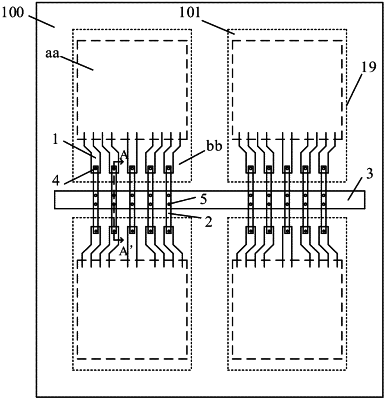
1. An array substrate, comprising a display region and a bonding region located outside the display region, the array substrate further comprising:
a bonding electrode, located in the bonding region and spaced apart from an outer edge of the bonding region, wherein part of the bonding electrode extends along a first direction parallel to a plane of the array substrate;
a base substrate and an active layer located on the base substrate, wherein an electrostatic barrier line and the active layer are provided in a same layer and made of a same material;
a source/drain metal layer and a gate metal layer located on the base substrate, wherein the bonding electrode and the source/drain metal layer are provided in a same layer and made of a same material; or the bonding electrode and the gate metal layer are provided in a same layer and made of a same material; and
the electrostatic barrier line, comprising one end electrically connected with a second end of the bonding electrode, and the other end extending to the outer edge of the bonding region, and resistivity of the electrostatic barrier line is larger than resistivity of the bonding electrode,
wherein the electrostatic barrier line is located outside the display region and on a side of the bonding electrode facing away from the display region, and the electrostatic barrier line is configured to prevent static electricity from entering inside of the array substrate from an edge of the array substrate,
wherein the electrostatic barrier line entirely extends along the first direction.
|